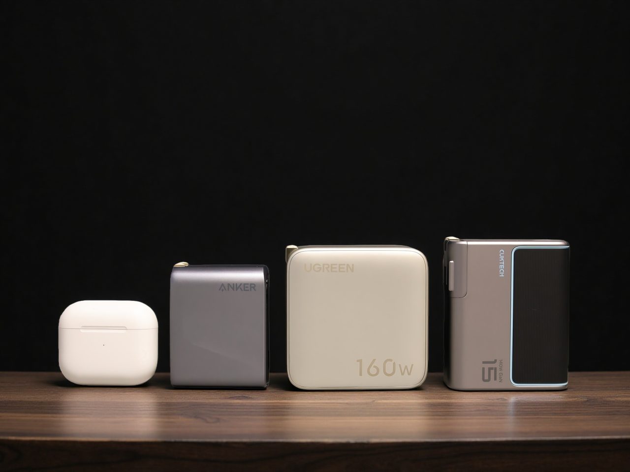
The difference between a GaN charger and a silicon charger comes down to the material used for the power device. GaN switches at far higher frequencies and tolerates higher voltages than silicon, so a charger of the same rating can be roughly half the size, run cooler and convert power more efficiently.
That shows up commercially as a higher unit price — a 65W GaN board in the region of ¥20–35, against ¥4–10 for a 20W silicon design — traded for a better customer experience and a lower return rate. The sections below set out the material-level differences and the sourcing logic that follows from them.
1. What GaN is: the difference starts at the material level
Mainstream charger designs use one of two families of power device: the conventional silicon (Si) MOSFET, or a gallium nitride power device. GaN is a wide-bandgap semiconductor, and compared with silicon it offers three physical advantages.
What that material difference means for a buyer rather than for a design team is the subject of GaN vs. silicon chargers.
- Higher switching frequency. GaN devices switch at more than ten times the frequency of silicon. The higher the frequency, the smaller the passive components — transformers and capacitors — have to be. Compact GaN chargers are a consequence of physics rather than of packaging ingenuity.
- Higher breakdown voltage and lower on-resistance. At an equivalent voltage rating, conduction losses are smaller, so less energy is thrown away during conversion.
- Better high-temperature behaviour. GaN derates far less than silicon as temperature rises. Combined with lower losses, this produces a clear drop in whole-unit heat.
2. GaN and silicon chargers in one table
| Dimension | GaN charger | Silicon charger |
|---|---|---|
| Volume at equal output | About 50% of the silicon equivalent | Larger; most obvious at 65W and above |
| Heat | Clearly lower; the housing stays warm rather than hot | Higher |
| Conversion efficiency | Higher, with lower no-load standby loss | Compliant but without an advantage |
| Power density | High; more power per unit of volume | Low |
| Bulk procurement reference price | Around ¥20–35 for a 65W unit | Around ¥4–10 for a 20W unit |
| Retail premium | Consumers will pay a premium for it | Heavily price-competed; thin margins |
| Typical application | Flagship fast charging, multi-port, portability | Entry configurations, cost-sensitive orders |
Price note: the figures above are indicative bulk procurement ranges. Actual cost depends on the PCBA design (the populated circuit board that makes up the charger), order volume and certification requirements.
3. What this means for a sourcing or product decision
Product line coverage
Where the downstream customer is a brand or a mid-to-premium retail channel, GaN is difficult to avoid. The sub-65W fast-charge market is converting to GaN quickly, and a trading company with no GaN line finds itself increasingly at a disadvantage in brand negotiations. Where the downstream channel is volume-driven and price-sensitive — convenience-store basics, for example — the cost advantage of silicon remains real. Most larger buyers run both lines in parallel rather than choosing one.
Price and margin structure
GaN carries a higher procurement price, but it also commands a higher retail price, and the gross margin band is wider than for silicon. At 65W, silicon retail pricing has already been compressed close to the floor, while 65W GaN still supports a visible premium at retail. For a buyer building a private label, the profit structure around GaN is the more favourable one.
Protocol configuration
GaN chargers are generally paired with newer protocol sets such as USB PD 3.0 and PPS, and protocol configuration determines which devices a unit can serve well. The common combinations in current supply are: PD 3.0 for Apple and most Android flagships, QC 3.0 for part of the Android market, PPS for Samsung, SCP for Huawei, and UFCS as the domestic unified fast-charge standard. On the manufacturing side these are configured in the PCBA solution, and a mature design can be made broadly compatible.
How those decisions surface in finished retail products is visible in Best GaN chargers in 2026.
4. Why GaN costs more
The question buyers ask most often is why a GaN charger costs so much more than a standard one. Unpacking the bill of materials, the premium sits in three places.
- The GaN power device itself. A single device costs several times a silicon part of the same rating. This is the dominant cost difference.
- More demanding design work. High-frequency operation complicates PCB layout and EMC treatment, and the engineering effort has to be amortised across the order.
- Certification testing. High power-density products attract stricter test programmes.
The trend is one-directional: GaN device cost is declining and adoption is rising. Buyers who establish a GaN line while the substitution is still underway capture the transition. Entering once prices have fully converged means competing in an already commoditised field.
The premium is a function of substrate and processing rather than of the element, which is abundant; gallium nitride is expensive to grow and to process, not to obtain.
5. A short procurement checklist
- Define the application before the wattage. Volume channels are usually better served by silicon at 20W; the GaN argument becomes decisive at 30W and above, and is strongest in 65W multi-port designs.
- Specify the protocol set explicitly. PD 3.0, QC 3.0, PPS, SCP and UFCS coverage should be written into the requirement rather than assumed from the PCBA platform.
- Ask for the power distribution table. On multi-port designs, the allocation scheme matters more than the headline total, and it is designed into the PCBA rather than added later.
- Confirm the certification set. CCC, CE, FCC, RoHS, PSE and KC are the usual baseline for cross-border channels, and the test programme for a high power-density product is more demanding than for a low-wattage one.
- Check the thermal design, not just the efficiency figure. GaN lowers losses; it does not remove the need for heat spreading.
- Model the margin at retail, not at cost. The GaN case rests on the retail premium, which is the figure that has historically held up.
Frequently asked
Is a GaN charger safe, and does low heat mean there is no overheating risk?
GaN reduces losses during normal operation. Every charger must still implement over-temperature, over-voltage, over-current and short-circuit protection; in most markets those four protections are a mandatory condition of certification. Buyers should verify the certification set rather than rely on the material claim.
Does a 20W charger need GaN?
Not necessarily. At 20W, the volume difference between silicon and GaN is small while the cost difference is clear, so silicon remains the more economic choice for volume channels. The GaN argument begins at 30W and is at its strongest in 65W multi-port products, where the volume advantage is largest.
Do multi-port chargers reduce speed when several devices are connected?
They share a fixed total. When several devices charge at once, power is allocated according to the design — a 65W dual-port unit typically splits as 45W + 20W. This is a property of the allocation scheme rather than a quality defect, and it is the reason the distribution table matters more than the headline wattage.